Photochemical etching has emerged as a highly effective process for creating intricate and high-precision components from a wide range of metals.
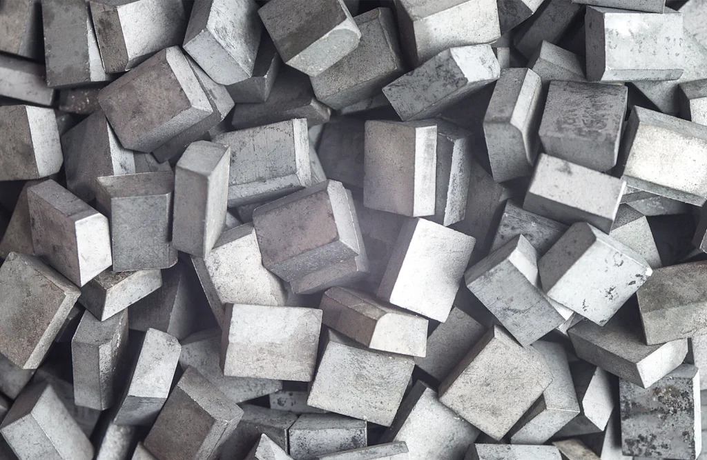
Renowned for its exceptional properties, tungsten has become one of the most popular materials for this innovative etching process, and it’s easy to see why. When paired with precision chemical etching, tungsten’s exceptional hardness, high melting point, and corrosion resistance make it ideal for creating durable tools and components that withstand even the harshest conditions.
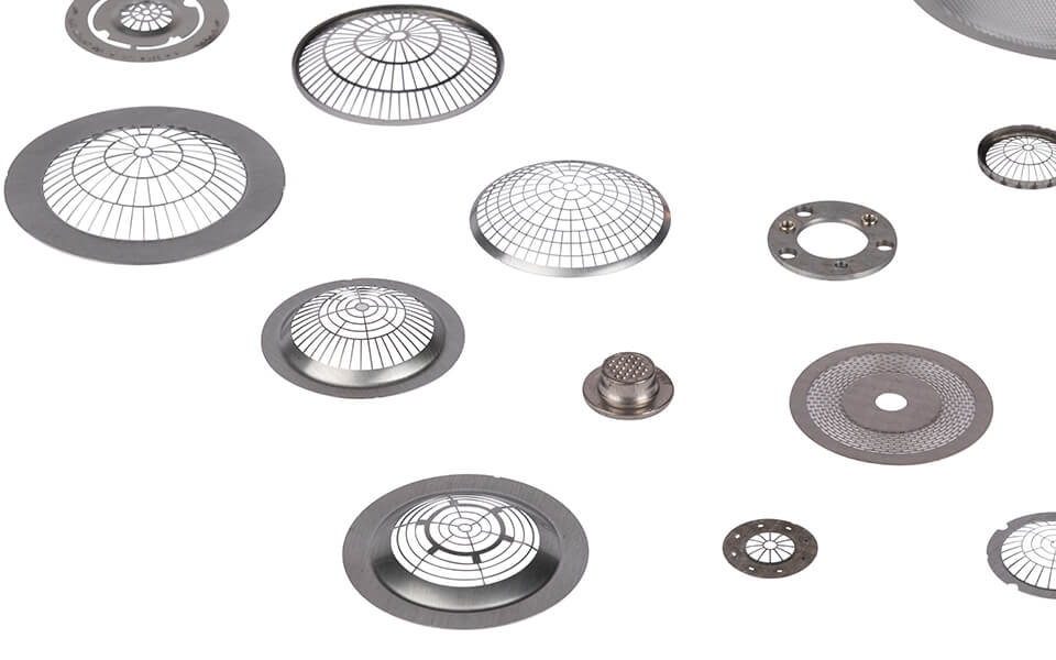
Leaders in chemical etching, E-Fab is renowned for delivering precision, reliable, and durable tungsten parts used by the world’s most important industries. Our specialized processes enhance the precision and quality of tungsten, producing precision tungsten parts for leading aerospace, semiconductor, microelectronics and medical companies.
This blog article explores the common use cases for photochemically etched tungsten, highlighting its applications across different industries and the advantages it offers.
What is Tungsten?
Tungsten, also known as Wolfram, is a refractory metal known for its exceptional properties, including the highest melting point of any metal (3422°C), superior strength, and high density. These qualities make tungsten an indispensable metal for applications where durability and reliability are paramount.
Tungsten’s superior corrosion resistance makes it highly durable in harsh environments, where it withstands exposure to corrosive substances better than many other metals. This property ensures long-lasting performance and reliability in critical applications such as aerospace, medical devices, and industrial tooling.
In its raw state, tungsten is a hard steel-gray metal that is often brittle and hard to work with. However, as an alloy, tungsten retains its impressive hardness, which exceeds that of many steels, and becomes malleable enough to be worked.
Notable Characteristics of Tungsten:
- Superior Corrosion Resistance: Tungsten remains intact when exposed to chemicals during the etching process, ensuring long-lasting durability in harsh environments.
- Extremely High Melting Point (3422°C): Ideal for applications that require materials to withstand very high temperatures.
- High Boiling Point: Used in applications like arc-welding electrodes and heating elements in high-temperature furnaces due to its outstanding ability to resist boiling.
- Low Thermal Expansion: Maintains its dimensions even under extreme temperature fluctuations, making it perfect for high-temperature applications.
- Low Volatility: Maintains stability at temperatures above 1,650°C, reducing the risk of vaporization.
- High Density (19.3 g/cm³): Effective for applications needing high mass and weight.
- Exceptional Hardness: Can endure significant stress, making it ideal for cutting tools and wear-resistant parts.
- Ductility: Can be shaped into various forms without cracking, enhancing its versatility.
- Excellent Thermal Conductivity: Efficiently conducts heat, suitable for applications requiring reliable heat dissipation.
- Non-toxic: Safe for use in medical devices and other applications requiring biocompatibility.
Tungsten’s combination of these properties, along with its ability to be intricately etched, makes it a versatile and reliable choice for various industries and specialized applications.
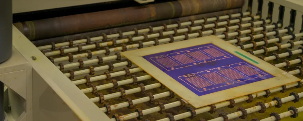
Overview of Photochemical Etching (PCE)
Photochemical etching (PCE) is a precise fabrication process used to create intricate metal parts, including those made of tungsten.
The process involves coating the metal with a light-sensitive photoresist, exposing it to ultraviolet light to pattern a design, and developing the exposed areas to reveal the desired pattern. The metal is then immersed in a chemical solution, often containing ferric chloride or another tungsten etchant, which selectively dissolves the unprotected areas.
This technique offers several advantages over traditional machining methods like CNC machining or lasering, as it allows for the creation of high-precision, intricate designs with precise features such as a consistent nose radius that are otherwise impossible.
Common Use Cases for PCE of Tungsten
Photochemically etched tungsten is a versatile and indispensable material relied on by some of the world’s leading industries. Its unique properties, combined with the precision and intricacy of the etching process, have seen it quickly become a preferred material in various high-performance applications. They include:
Medical Devices
Photochemically etched tungsten is extensively used in the medical field due to its biocompatibility and ability to withstand sterilization processes. Tungsten components are crucial in the manufacturing of intricate parts for medical devices such as endoscopic instruments, surgical blades, and ablation devices.
The high density of photochemically etched tungsten is effective at blocking radiation, making it ideal for producing radiation shields. These shields are essential components in medical imaging and radiation therapy equipment, providing reliable protection against harmful radiation.
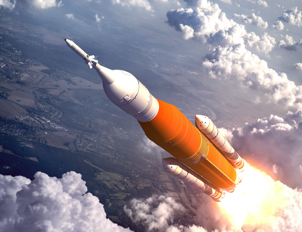
Aerospace and Defense Components
In the aerospace and defense industries, it’s crucial that the materials used perform under extreme conditions. With its high melting point, density, and high tensile strength, it’s little wonder why tungsten is the popular choice for various applications across these sectors.
With its incredibly high melting point (3422°C) and excellent thermal stability, photochemically etched tungsten is used in the production of components that must withstand extreme temperatures, such as rocket nozzles, satellite parts, and heat shields. Tungsten’s fine grain size ensures that these components have the necessary strength and durability.
Tungsten’s high density also makes it the perfect metal for producing weight-balancing components critical for aerospace applications. These compact and efficient counterweights and ballast components are crucial for maintaining balance and stability in aircraft and spacecraft.
Electronics
In the electronics industry, the miniaturization of components is a continuous trend. Tungsten’s excellent electrical conductivity and ability to maintain structural integrity at micro scales have made it the clear material choice and a range of electronic applications.
Photochemically etched tungsten is used in the production of everything from microelectromechanical systems (MEMS) to semiconductor components and connectors.
Due to its superior thermal and electrical conductivity, tungsten is also a popular material choice for electron guns used in electronic devices, where precision and efficiency are essential. Its high-temperature resistance and durability, on the other hand, make tungsten a proven choice for components in X-ray generation equipment, ensuring reliability and performance in medical and industrial imaging. Additionally, tungsten is used in control grids for traveling wave tubes (TWTs), which are vital components in microwave and satellite communication systems. For more information on TWTs, read “What are traveling wave tubes?‘
E-Fab’s Expertise in Tungsten Etching
Here at E-Fab, we’re experts at etching and forming tungsten to precise standards and specifications.
As an industry leader in delivering innovative, accurate, and reliable tungsten parts, we’ve positioned ourselves as the trusted manufacturing partner for leading industries across the globe. Our innovative etching process enables us to deliver parts with complex or intricate geometries and tight tolerances for applications in some of the harshest environments.
We etch many grades of tungsten, including high-purity, copper-tungsten, tungsten-rhenium, thoriated rhenium, and AKS-grade.
We take pride in our commitment to excellence and ensuring the highest quality standards throughout our manufacturing processes. To achieve this, we hold compliance certifications (ITAR, AS9100, ISO 9001:2015, CMRT), highlighting our dedication to best practices and delivering top-notch products to our customers.
A Proven Metal for Applications that Demand Performance
From medical devices and aerospace components to electronic parts and industrial tooling, photochemically etched tungsten continues to play a critical role in advancing technology and enhancing performance.
As manufacturing technologies evolve, the use cases for photochemically etched tungsten are only set to expand, making it even more important to find a proven manufacturing partner with the experience and expertise needed to deliver precision etched tungsten parts guaranteed to perform.
If you’re looking for a proven manufacturing partner to deliver tungsten components you can rely on in even the harshest environments, the team at E-Fab can help. Thanks to decades of experience and expertise in a suite of processes, we’re an industry leader in delivering innovative, accurate, and reliable parts.