
When you’re in the business of modern technology, you need to know that your semiconductor components have the quality, innovation, and reliability required to perform.
With your choice of who produces your components significantly impacting the final product’s performance and efficiency, choosing the right manufacturing partner becomes paramount.
E-Fab is a leading photochemical etching manufacturer specializing in manufacturing components for semiconductors and semiconductor fabrication equipment. Renowned for our industry-leading expertise in precision metal etching, E-Fab has become the trusted partner for semiconductor manufacturing across a wide range of sectors. Driven by innovation and precision, our advanced etching process precisely fabricates intricate components critical to semiconductor technology.
In this article, we explain what to look for in a semiconductor manufacturer, the power of the photochemical etching process, and the reasons E-Fab has led the way in precision semiconductor component manufacturing.
The Importance of Precision and Quality in Semiconductor Manufacturing
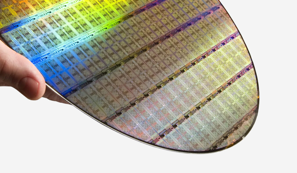
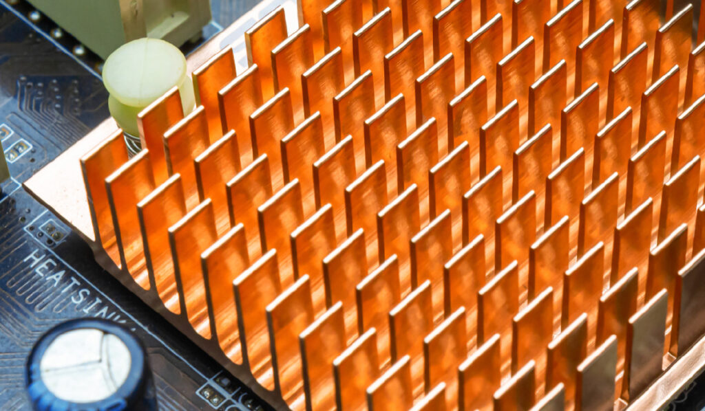
Semiconductor components are the heart of modern electronic devices. From smartphones to medical equipment, aerospace technology to consumer electronics, these intricate components deliver performance and reliability across key areas of our everyday lives.
In semiconductor manufacturing, precision and quality are essential to ensuring the performance and reliability of the final products. Techniques like plasma etching and wet etching are employed to achieve the intricate patterns required on silicon wafers, which form the foundation of semiconductor wafers used in various applications.
High-quality semiconductor production relies on advanced semiconductor equipment to maintain tight tolerances and minimize defects, which is crucial for the functionality of components such as semiconductor diodes, transistors, and integrated circuits. Any deviation in precision can lead to significant performance issues, emphasizing the need for stringent quality control throughout the manufacturing process.
The manufacturing partner you choose must have a proven track record of delivering high-precision components that meet stringent industry standards.
Semiconductor Parts and Materials
Semiconductor parts and materials are the building blocks of modern electronic devices, encompassing a wide range of components and substances essential for their function.
Key semiconductor materials include silicon, which is processed into silicon wafers, and other semiconductor materials like copper, stainless steel, and nickel alloys. These materials are meticulously fabricated into semiconductor wafers through processes like doping, lithography, and etching. Critical parts, such as transistors, diodes, and integrated circuits, are then formed on these wafers.
Each component requires precision manufacturing to ensure optimal performance, reliability, and efficiency in applications ranging from consumer electronics to advanced computing systems.
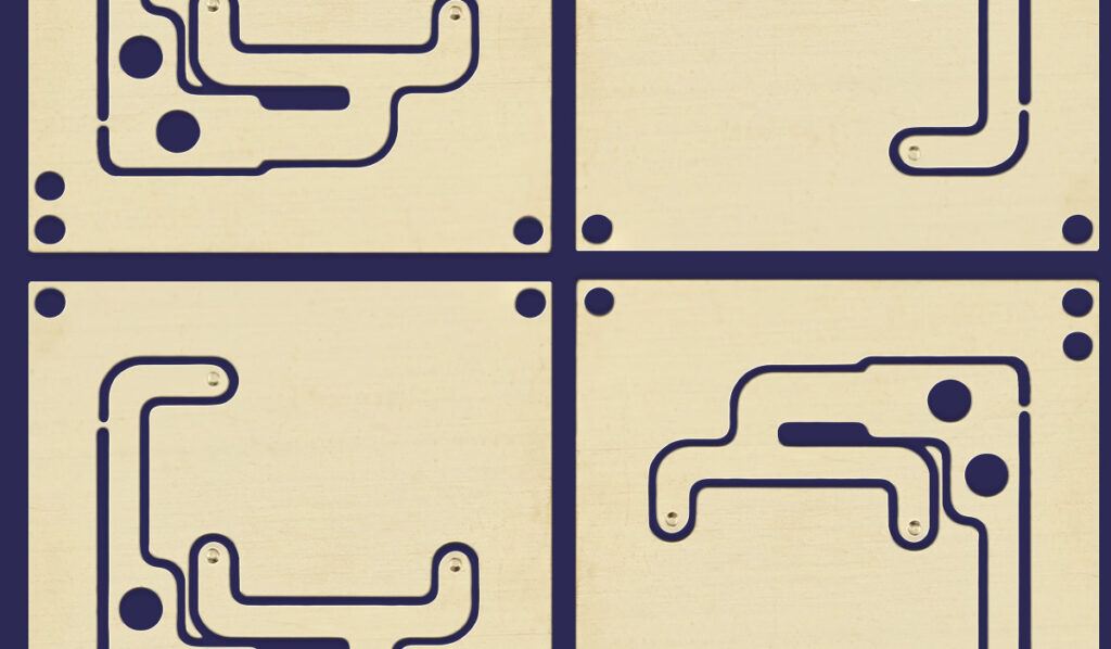
E-Fab has almost 40 years of experience fabricating a wide variety of semiconductor parts, such as contacts, maps, splits, apertures, clips, springs, connectors, EMI/RFI shielding, and much more. We can produce nearly any size feature with tight tolerances so long as it is not smaller than the material thickness. For example, we can produce precision micro bumps as small as 0.004″ ±0.001″ in diameter with a max. height of 0.001″ ±0.0005″. We can achieve these minimum constraints on materials, such as copper and brass alloys, SST, and others, less than 0.005″ thick.
We can design, prototype, and produce a custom photo-etched carrier from the following semiconductor materials:
- Copper
- Nickel Alloys
- Stainless Steel
- Beryllium Copper
Our semiconductor components are used in a wide range of applications and industries, including electronics, aerospace, medical, military and defense, computers, energy, communication, and more.
Different Types of Semiconductor Manufacturing Equipment
- Semiconductor Design Equipment
Semiconductor design equipment consists of specialized CAD software developed for circuit and pattern design. This software allows engineers to create detailed schematics and layouts essential for the subsequent manufacturing stages, ensuring the precision needed for complex semiconductor components, such as a semiconductor diode.
- Photomask Manufacturing Equipment
A photomask, or glass dry plate, is a glass or quartz plate on which the original pattern plates used in the manufacturing process of electronic circuit components are formed. Photomask manufacturing equipment deposits a light-shielding material, such as chrome, onto a glass substrate and draws the circuit pattern using laser equipment or an electron beam. This process also involves developers, dry etching equipment, and inspection equipment to ensure precision and accuracy.
- Wafer Fabrication Equipment
Wafer fabrication begins with ultra-high purity silicon single-crystal ingots, which are cut into thin wafers using diamond blades. These silicon wafers are then polished and placed in a high-temperature oxidation furnace to create an oxide film. A photosensitive agent called photoresist is applied to the silicon wafer surface using a resist coater/developer. Circuit patterns are formed by scaling and burning photomask images onto the wafer using semiconductor exposure systems. Unnecessary oxide film and resist are removed through etching and stripping. Ion implantation and annealing equipment introduce substances like boron and phosphorus into the wafers, making them semiconductors. The wafers are then placed in a plasma system, where inert gas plasma forms an aluminum metal film for electrode wiring. Finally, wafers are tested chip by chip to identify defects, completing this stage of the process.
- Processing Equipment for the Wafer Process
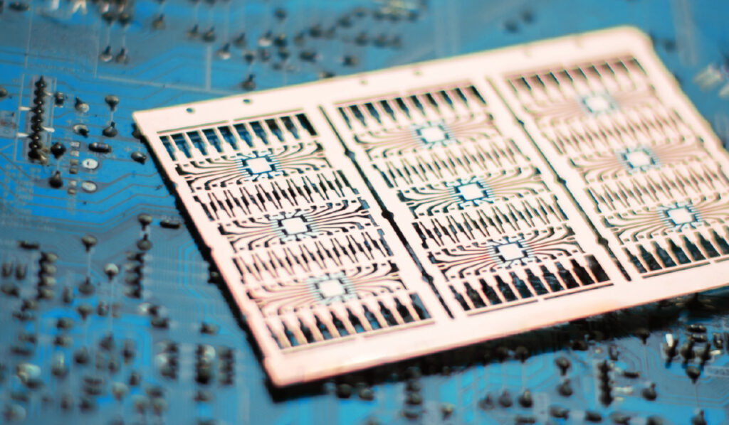
In the back-end process, wafers are cut and separated into individual chips using dicing saw equipment. These chips are then fixed in place on lead frames, ready for further assembly.
- Assembly Equipment
Assembly equipment involves multiple stages to create the final semiconductor product. First, die bonder equipment connects the chips to the lead frame using bonding wire. Next, the chips are packaged with resin using molding devices for protection. Individual semiconductor products are then cut and separated from the lead frames using a die, and the external leads are formed into their final shape.
- Inspection Equipment
Inspection equipment is used to identify and exclude defective products. An accelerated temperature-voltage stress test, known as burn-in, is performed alongside functional tests to detect initial defects. Further electrical characteristic tests and visual structural inspections ensure that defective products are removed. Additionally, reliability tests such as environmental tests and long-term life tests are conducted to guarantee the durability and performance of the semiconductor products.
These various types of semiconductor manufacturing equipment work together to produce high-quality, reliable semiconductor components essential for a wide range of electronic devices. This comprehensive approach ensures that every stage of semiconductor machinery manufacturing meets the highest standards, providing the precision and reliability necessary for advanced technologies.
Key Considerations When Choosing a Manufacturing Partner for Semiconductor Devices
Choosing the right manufacturing partner for semiconductor components is crucial to ensure you receive the highest levels of quality and precision. A reliable partner with advanced technological capabilities and industry expertise can significantly enhance the performance and durability of semiconductor products, ensuring they meet stringent industry standards and perform reliably in even the most demanding applications.
Here are the key considerations to keep in mind when choosing a manufacturing partner for your semiconductor components:
1. Quality and Precision
The semiconductor industry is built on quality and precision. It’s important that you partner with a manufacturer with a proven track record of delivering components with exceptional accuracy and consistency. They must be able to deliver components that perform as intended, with minimal defects and variations. This level of quality is essential for maintaining the integrity and reliability of electronic devices, which rely on precise and consistent semiconductor components.
To assess a potential partner’s commitment to quality, look for certifications such as ISO 9001, which indicates adherence to international quality management standards. Additionally, inquire about their quality control processes, including inspection and testing procedures, to ensure they meet the stringent requirements of the semiconductor industry.
2. Technological Capabilities
The semiconductor industry is constantly evolving, with advancements in materials, processes, and technologies. A manufacturing partner must have state-of-the-art equipment and facilities to keep pace with these developments.
Advanced technological capabilities enable the production of complex and high-precision semiconductor components. This includes the ability to handle cutting-edge materials, utilize sophisticated manufacturing processes, and implement automation and robotics for improved efficiency and accuracy. Evaluate the partner’s investment in research and development, as this indicates their commitment to staying at the forefront of technological advancements.
3. Industry Experience and Expertise
A partner located in Silicon Valley, with a deep understanding of semiconductor manufacturing, can navigate the complexities of the industry and anticipate potential challenges. Their proximity to the heart of tech innovation ensures they are well-versed in the intricacies of the production process, from design and prototyping to mass production.
Look for a partner with a proven track record of successfully manufacturing semiconductor components for various applications. Their expertise should encompass knowledge of industry-specific requirements, standards, and best practices. Additionally, consider their experience working with other companies in your sector, as this indicates their ability to meet your specific needs.
4. Customization and Flexibility
The semiconductor industry often requires customized solutions to meet specific design and performance requirements. A manufacturing partner should offer a high degree of customization and flexibility in their services. This includes the ability to tailor manufacturing processes, materials, and designs to meet your unique specifications.
Flexibility is also essential in adapting to changing demands and project requirements. A partner that can quickly adjust production schedules, scale up or down as needed, and accommodate design changes ensures that your projects remain on track and within budget. Evaluate the partner’s ability to provide personalized solutions and their willingness to collaborate closely with your team.
5. Reliability and Consistency
A dependable partner ensures that every batch of components meets high standards of quality and performance. Consistency in production processes minimizes variations and defects, resulting in reliable and high-performing semiconductor components.
Assess the partner’s track record for on-time delivery, adherence to specifications, and their ability to maintain consistent quality across large production runs. Reliability also extends to their customer support and communication. A partner that provides transparent and responsive communication ensures that any issues or concerns are promptly addressed.
6. Compliance with Industry Standards
Compliance with industry standards is non-negotiable in semiconductor manufacturing. Manufacturers must adhere to relevant regulatory requirements, industry standards, and certifications to ensure the safety, reliability, and quality of the components. This includes compliance with standards such as ISO 9001 for quality management, ISO 14001 for environmental management, and industry-specific standards like IPC for electronic components.
Evaluate the partner’s commitment to maintaining and updating their certifications and their ability to meet the regulatory requirements of different markets. Compliance with industry standards demonstrates their dedication to quality and their ability to meet the rigorous demands of the semiconductor industry.
E-Fab – Semiconductor Manufacturing Specialists
Pioneers in photochemical etching, E-Fab has become a proven partner for semiconductor manufacturing due to our ability to deliver intricate and precise patterns essential for manufacturing semiconductor components.
Boasting industry-leading equipment and technology, we can meet the demand for precise, complex, and feature-rich metal semiconductor parts and components with the highest levels of accuracy and repeatability which is of vital importance due to the critical nature of semiconductor applications.
Our precision photochemical etching process and industry-leading equipment in our ISO 9001:2015 certified facility ensure that every component we fabricate is of the highest quality.
Our knowledgeable engineers will work with you to help you realize your semiconductor part or component, no matter the complexity. Because chemical etching does not increase as part complexity increases, our engineers can focus on optimizing part functionality and achieving high repeatability, uniformity, and consistent production quality.
Our precision photochemical etching capabilities offer the following key advantages for delivering semiconductor parts and components:
- Burr-free and stress-free semiconductor parts
- Tight, low tolerances for small feature sizes with a high level of consistency and repeatability.
- Achieve intricate shapes, complex geometries, and 3D feature profiles that are impossible with other machining processes.
- Photochemically etched parts can be produced at high volumes with exacting uniformity, which reduces time to market and saves on production costs.
- Allows us to work with a wide range of metal substrates that would either be too conductive, fragile, or hard to form or work with using other machining methods.
- Allows for unparalleled repeatability and scalability of uniform etching of almost any metal substrate or materials used in manufacturing semiconductor parts and components.
Ensuring Precision and Reliability in Semiconductor Devices
In the fast-moving semiconductor industry, a strong manufacturing partnership is your key to staying competitive and delivering top-quality products to the market.
By prioritizing precision, reliability, innovation, flexibility, and industry-specific expertise, you can find a partner who not only meets your current needs but also supports your long-term growth and success.
If you need a proven partner for your precision semiconductor manufacturing, the team at E-Fab is here to help. With decades of experience, E-Fab has built a reputation for delivering high-quality, reliable, and innovative solutions that meet the stringent demands of the semiconductor industry.
Our precision semiconductor photo etching services produce intricate and complex parts and components that achieve ultra-precise dimensional and structural tolerances and high conductivity for long service life and improved yields.
Our knowledgeable team works with you at every step of the project, from consultation to design to manufacturing to delivery, and provides high-quality product solutions that precisely satisfy your requirements.