
In semiconductor manufacturing, precision and quality are essential to ensuring the performance and reliability of the final product.
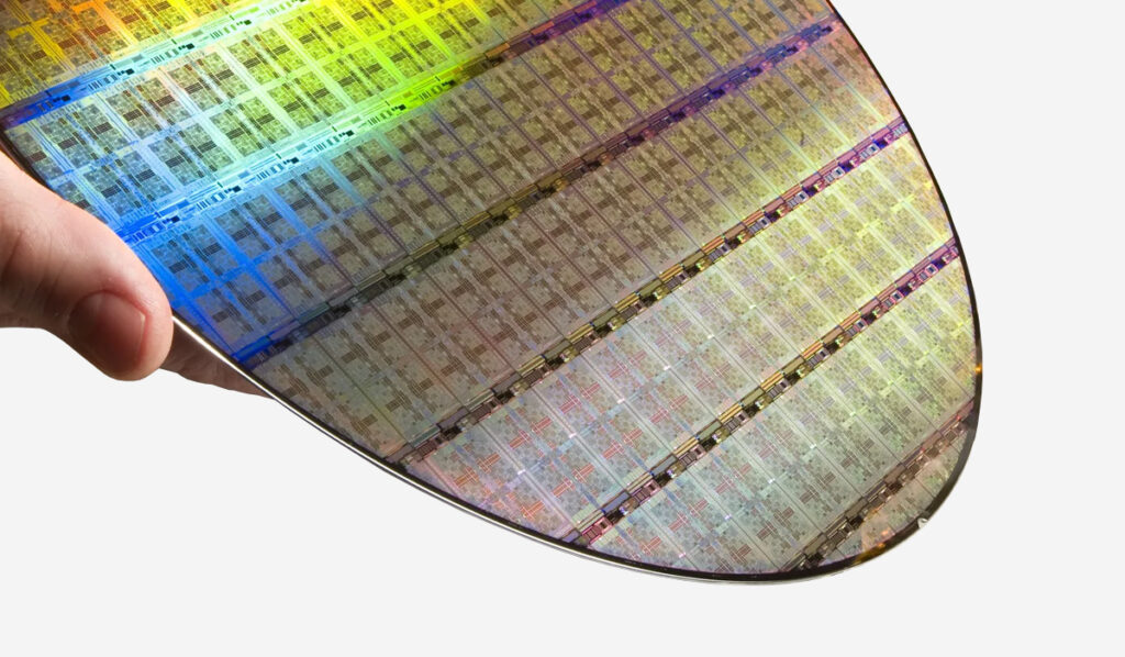
With the functionality of critical electronic devices on the line, you need a manufacturing process with high precision and control, as even the slightest deviation can lead to failure. The heart of these devices is the semiconductor, a thin microelectronic composed of several components created out of silicon, germanium, and metals.
Let’s look at the process of semiconductor manufacturing and how photochemical etching plays a part in creating the thin metal parts found in today’s semiconductors.
With a fast turn-around time, this etching process produces parts with exceptionally tight dimensional tolerances, free from burrs, sharp edges, or the need for further finishing. A cheaper alternative to traditional machining methods, it also offers the added benefit of easily making changes and adjustments during production.
Renowned for our industry-leading expertise in precision metal etching, E-Fab has become the trusted partner for semiconductor part manufacturing. Driven by innovation and precision, our advanced photochemical process precisely fabricates intricate components that are powering modern technology.
As we dive deeper, we’ll explore the semiconductor etching process, its key applications, advantages, and importance in producing high-quality components for the industry.
What is Photochemical Etching?
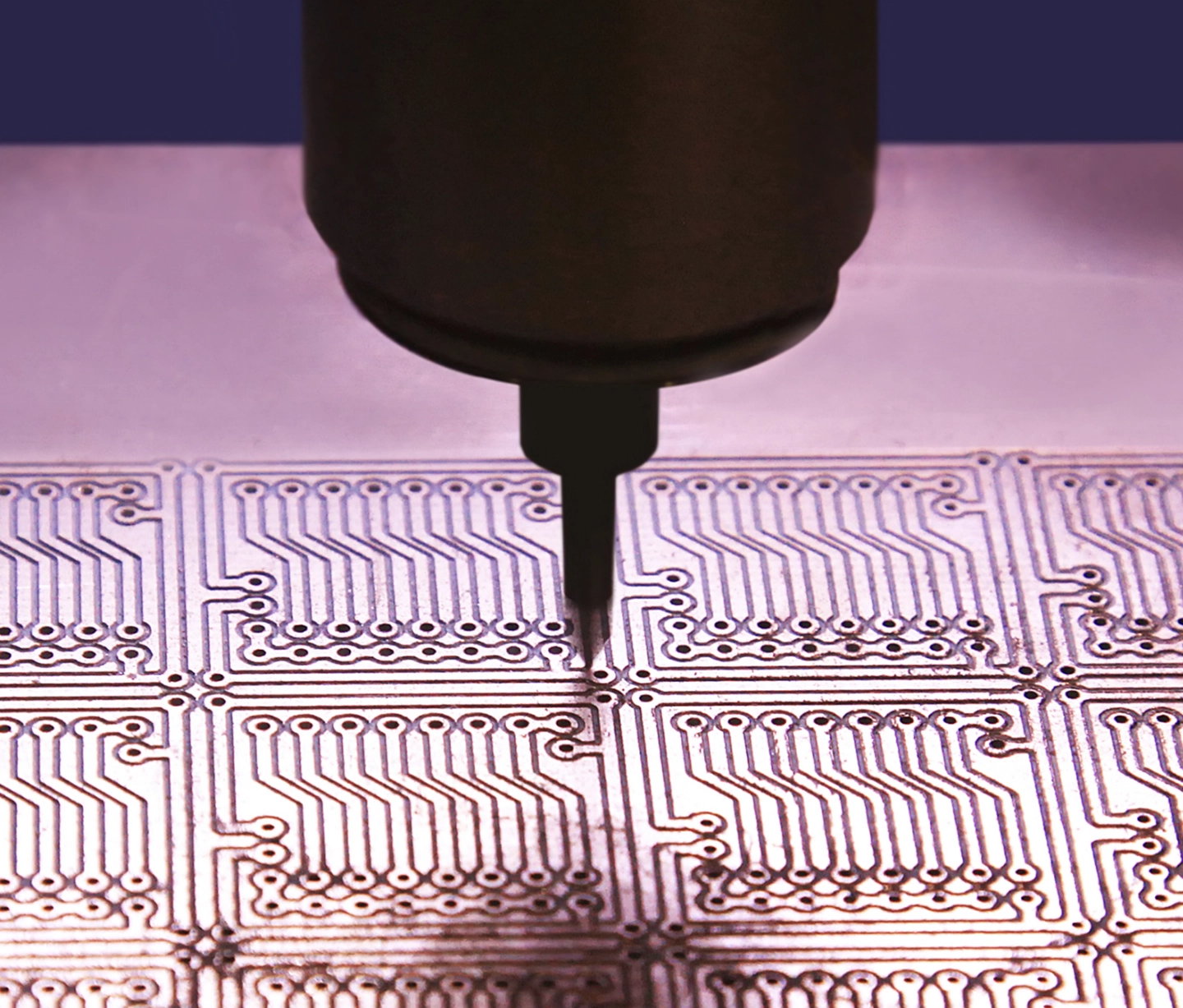
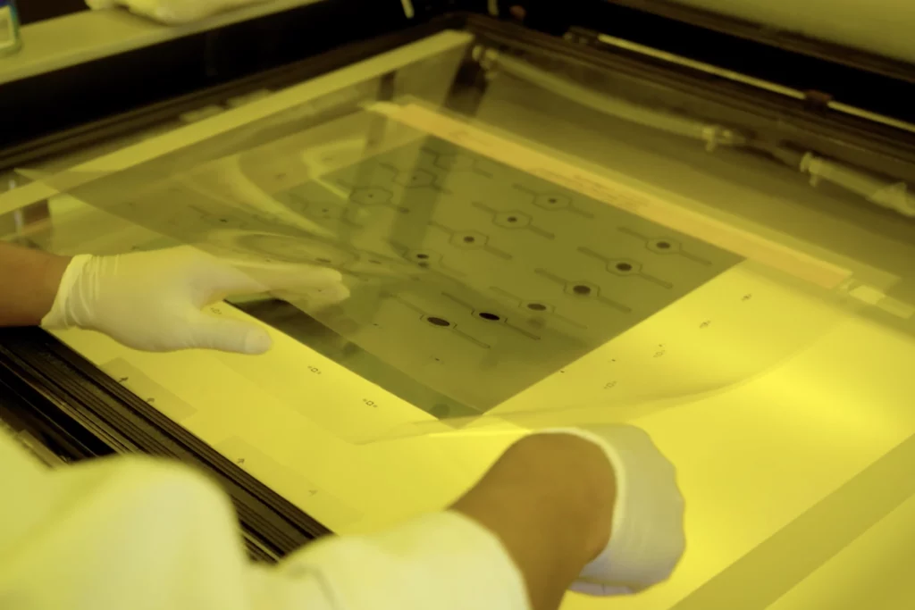
Photochemical etching, also referred to as chemical milling or photo-etching, is a subtractive manufacturing technique that employs light-sensitive photoresist masks and chemical solutions to meticulously remove material and form intricate patterns on metal surfaces. The process starts with applying a photoresist layer onto the metal, which is then exposed to UV light through a patterned mask. The exposed sections become soluble, allowing the chemical etchant to dissolve the metal, thus creating the desired shapes or features.
This technique is highly effective for producing intricate and complex designs with tight tolerances, making it ideal for semiconductor applications where precision is critical.
One of the primary advantages of chemical etching over traditional machining methods is its versatility. Unlike mechanical etching or laser cutting, it can be used on a diverse range of metals, including stainless steel, copper, aluminum, and titanium, without causing thermal stress or distortion.
Chemical etching is also a cost-effective solution for high-volume production, as it eliminates the need for expensive tooling and setup costs associated with conventional machining methods.
Dry Etching vs Wet Etching
Wet etching and dry etching are crucial techniques applied in semiconductor component manufacturing.
Wet etching involves chemical solutions to remove material and is effective for isotropic etching, where the etch rate is uniform in all directions. It’s a simple and cost-effective technique, but it lacks the precision required for intricate patterns and can lead to undercutting.
Dry etching, which includes methods such as plasma etching, reactive ion etching, and ion beam etching, uses gasses and plasma to etch materials. Dry etching allows for anisotropic etching, providing precise, directional etching critical for creating detailed semiconductor devices. While dry etch techniques offer superior control and accuracy, they are generally more complex and expensive than wet etching.
The Semiconductor Etching Process
As a precise and versatile manufacturing process, photochemical etching is used to produce intricate and complex semiconductor components.
The key steps of the photochemical etching process include:
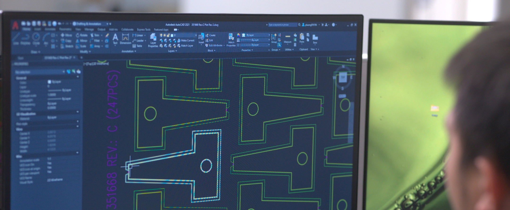
Design and Phototool Creation
- Design Preparation: Designing the semiconductor component begins with a detailed drawing. In most cases, CAD software is used to create this design, ensuring that all dimensions and tolerances are specified to meet the exact requirements of the component.
Material Selection and Cleaning
- Material Selection: The appropriate metal substrate is chosen based on the specifications of the semiconductor component. Some of the common materials used include copper, aluminum, nickel, and other alloys, which are selected for their electrical properties, thermal stability, and compatibility with semiconductor applications.
- Cleaning: The metal sheets are then thoroughly cleaned to remove any contaminants such as oils, dirt, or oxidation. This cleaning step is critical to ensure proper adhesion of the photoresist layer and to achieve uniform etching.
Photoresist Application
- Coating: A light-sensitive photoresist layer is applied to clean metal sheets. This coating is typically applied using a spin coating or lamination process to ensure a uniform thickness.
- Drying: The photoresist is then dried to solidify the coating, making it ready for exposure to UV light.
Exposure and Development
- Digitally Image Design: The design is loaded onto a UV laser digital imaging tool, which transfers the design to the photoresist laminated on the metal sheet.
- Development: The exposed metal sheet is then placed in a developer solution, which washes away the soluble photoresist, leaving the pattern of the design on the metal. The unexposed areas are protected by the remaining photoresist, creating a mask for the etching process.
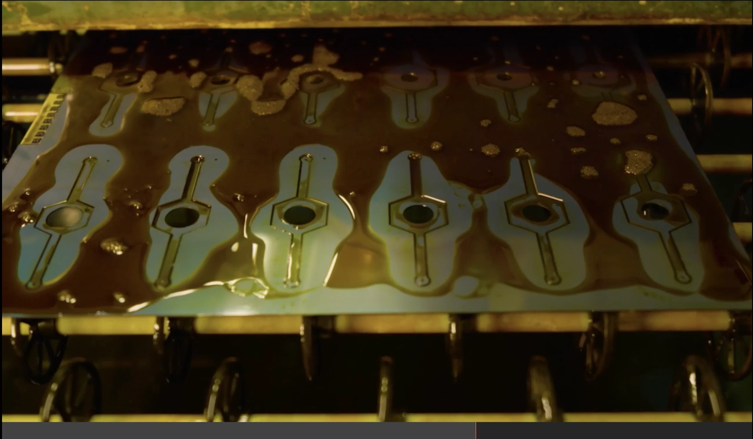
Etching
- Chemical Etching: The developed metal sheet rolls through our etchers, which spray a chemical etchant solution. The spraying is done at high pressure, etching away all the material not protected by the photoresist. Some of the chemical etchants used in the process include ferric chloride for iron-based metals or cupric chloride for copper. The etching process is closely monitored to ensure that the desired depth and precision are achieved without undercutting or over-etching.
- Inspection: After etching, the component is thoroughly inspected to ensure that all features have been accurately produced according to the design specifications. This step is critical in semiconductor manufacturing, where even minute deviations can affect performance.
Stripping and Final Cleaning
- Photoresist Stripping: As the remaining photoresist is stripped away, the final etched pattern is revealed. In most cases, this is done with the use of a chemical solution or a plasma cleaning process.
- Final Cleaning: The etched metal component undergoes a final cleaning to remove any residual chemicals or debris. This ensures that the component is free of contaminants that could interfere with its performance in semiconductor applications.
Finishing and Quality Control
- Surface Treatment: Depending on the application, the etched components may undergo additional surface treatments, such as passivation, plating, or coating, to enhance their durability, electrical conductivity, or corrosion resistance.
- Quality Control: The final components are subjected to rigorous quality control inspections, including dimensional checks, visual inspections, and functional testing. This ensures that each semiconductor component meets the required standards for precision, performance, and reliability.
Key Factors Influencing Etching Quality and Precision
When fabricating semiconductor components, it’s critical to control several variables carefully during the photochemical etching process.
1. Mask Alignment Accuracy: Precise alignment of the photomask is critical to ensure the pattern is transferred correctly.
2. Photoresist Quality: The type and quality of photoresist, along with its application uniformity, influence the sharpness and fidelity of the pattern.
3. Etchant Concentration: The concentration of the etchant solution determines the aggressiveness of the etching process and directly impacts the quality of the etched features. A balanced concentration is needed to achieve precise and controlled etching without damaging the material.
4. Exposure Time and Etch Rate: The duration of exposure to the etchant must be carefully controlled. Too short an exposure may result in incomplete etching, while too long can cause excessive material removal and reduce the fidelity of intricate patterns.
5. Masking Technique: The quality of the masking layer used to protect unetched areas is vital. Any defects or inconsistencies in the mask can lead to unwanted etching in protected areas, affecting the final quality of the component.
6. Temperature: The temperature of the etchant solution can influence the rate of the chemical reaction and, consequently, the etching process.
7. Material Properties: Different materials react differently to etchants, and factors such as the material’s hardness, grain structure, and chemical composition can impact the uniformity and accuracy of the etching.
For instance:
Hardness: Harder materials may resist etching more than softer ones, leading to slower etch rates and the potential for uneven etching.
Grain Structure: Fine-grained materials generally etch more uniformly than coarse-grained materials, which can lead to surface roughness and inconsistencies.
Chemical Composition: The composition of the material can affect how the etchant interacts with it. Some metals may form protective oxide layers during etching, which can slow down the process and impact precision.
Learn about the materials we etch for metal components for semiconductors.
8. Process Control: Consistent monitoring and control of all process parameters (e.g., gas flow rates, chamber pressure, RF power) are essential for repeatability and precision.
When you carefully manage these steps and factors, you’ll be able to manufacture the highly precise and intricate patterns required for advanced semiconductor fabrication.
Advantages of E-Fab’s Advanced Etching Techniques for Semiconductor Components
Providing exceptional precision and accuracy, E-Fab’s innovative photochemical etching process creates finely detailed semiconductor components with tight tolerances and delivers enhanced component integrity by minimizing stress on the material and ensuring burr-free edges.
Our ability to create complex geometries and microstructures with uniform precision ensures that each component meets the stringent specifications required for a wide range of critical semiconductor applications.
The main advantages of E-Fab’s precision photochemical etching process include:
- High Precision and Resolution: We’re capable of creating extremely fine and intricate patterns with high accuracy, essential for advanced semiconductor devices.
- Flexibility in Design: The innovative process allows for complex and customized designs that are difficult to achieve with other etching methods.
- Cost-Effective: Our proven process reduces material waste and can be conducted in batch processes, lowering overall production costs.
- Wide Material Compatibility: PCE is suitable for a variety of materials used in semiconductor manufacturing, including metals and alloys.
Applications in the Semiconductor Industry
Allowing for the fabrication of finely detailed metal components with exceptional precision, the chemical etching process is widely used for producing high-precision components across many industries and applications.
Some of the main semiconductor applications etched components are used for include:
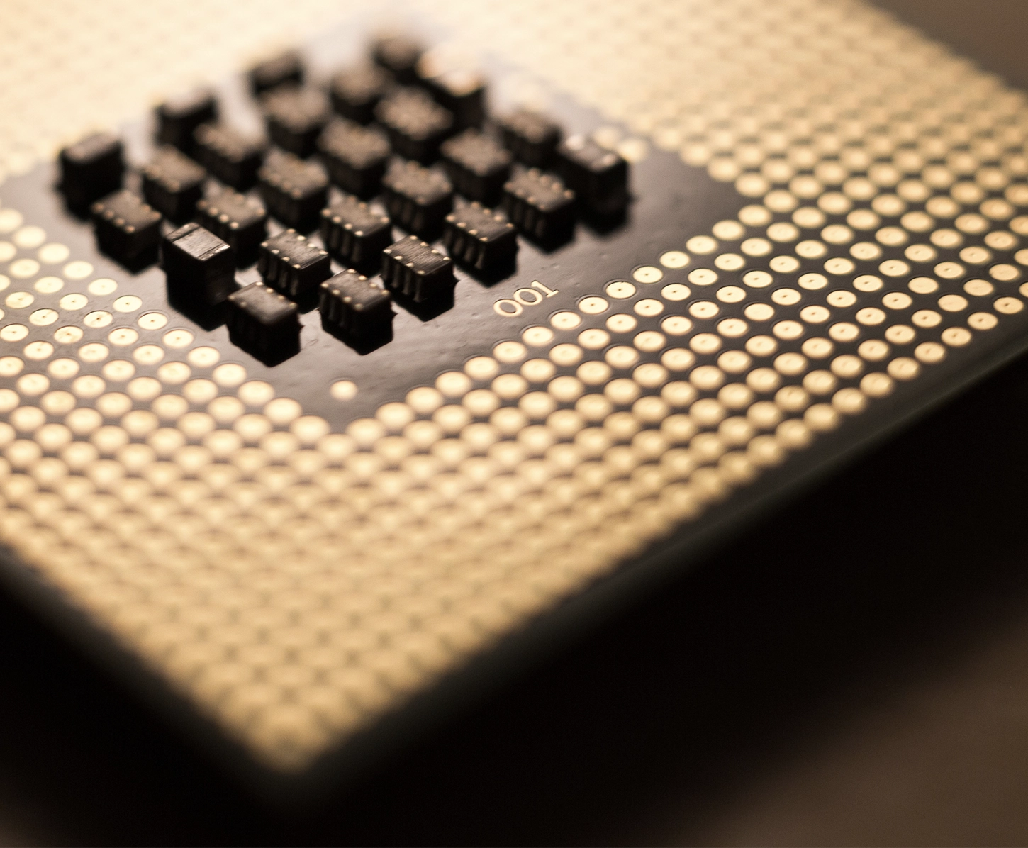
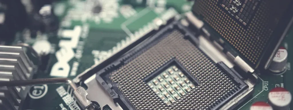
Microprocessors, Microelectronics and Integrated Circuits
Etching is fundamental in the fabrication of microprocessors and integrated circuits (ICs), both of which require extremely fine and precise patterns to function correctly. Through photochemical etching, it is possible to create complex circuits and transistors that enable the production of high-performance microprocessors, ICs and microelectronics for cars, planes, and space exploration vehicles.
MEMS Devices
Microelectromechanical systems (MEMS) devices, which include sensors, actuators, and other miniature mechanical components, rely heavily on etching for their fabrication. The precise removal of the material allows for the creation of intricate mechanical structures that are crucial for their functionality.
Photonic Devices
Photonic devices, such as lasers, modulators, and detectors, also depend on precise etching techniques. These devices require exact dimensions and smooth surfaces to operate efficiently. Etching processes are used to create waveguides, mirrors, and other optical components with the necessary precision.
Advanced Packaging
A number of advanced packaging techniques, like through-silicon vias (TSVs) and flip-chip technology, rely on the photochemical etching process for reliability and functionality. The etching forms the necessary channels and connections in these advanced packaging methods, creating interconnections and features that enable higher performance and miniaturization. Photochemical etching is also a cost-effective method to manufacture microelectronic lids.
Compound Semiconductors
Etching is also vital in the production of compound semiconductors, which are used in high-frequency and high-power applications. The ability to etch materials like gallium arsenide (GaAs) and silicon carbide (SiC) with precision allows for the development of components that can operate under extreme conditions.
Leading the Way in Precision Photochemical Etching
The photochemical etching process has become essential for the development of advanced electronic devices because it can create intricate patterns and structures with high accuracy.
From microprocessors and MEMS devices to photonic components and advanced packaging, this advanced etching process ensures the functionality and performance of modern technology across the semiconductor industry. As technology continues to evolve at a rapid rate, manufacturers will continue to rely on PCE to produce high-quality semiconductor components that meet the industry’s demanding requirements.
E-Fab is a leading photochemical etching manufacturer specializing in semiconductor machinery manufacturing.
As an ISO 9001:2015 and ITAR certified company, we offer a unique combination of advanced technology, proven production processes, engineering expertise, and value-added secondary services, allowing us to provide innovative solutions to complex jobs and unique design challenges for semiconductor parts and components.