
In the rapidly evolving field of electronics, the quality of semiconductor components is critical to ensuring the performance, safety, and reliability of electronic devices and systems across a wide range of industries.
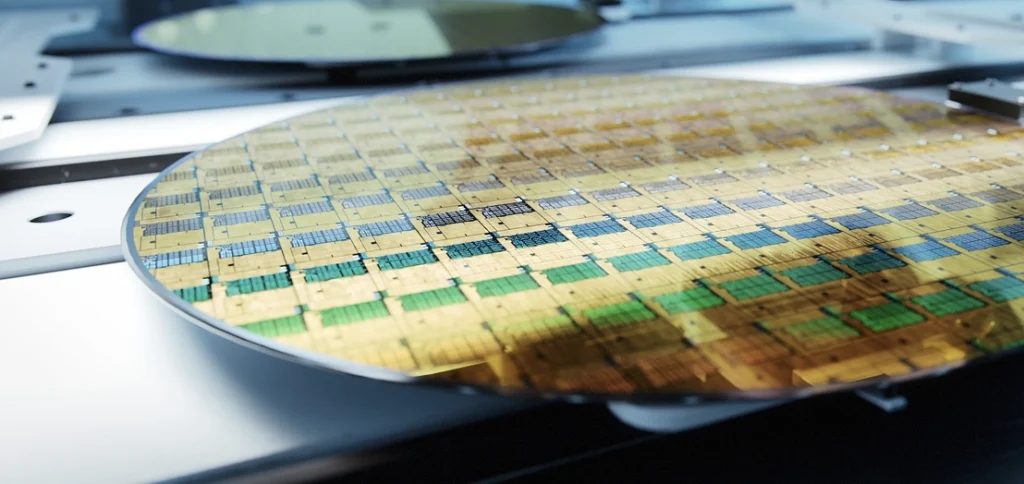
The tiny, intricate parts found in semiconductors are the backbone of modern technology, powering everything from smartphones to advanced computing systems. Photochemical etching (PCE) offers manufacturers precise and reliable thin metal parts with extremely tight tolerances and intricate geometries for high-quality semiconductor components.
Renowned for our industry-leading expertise in precision metal etching, E-Fab has become the trusted partner for semiconductor part manufacturing across a wide range of sectors. Driven by innovation and precision, our advanced photochemical process precisely fabricates intricate components critical to the semiconductor market.
In this article, we explore the photochemical etching process, its benefits, and how this innovative process improves the quality of electronic components and advances the electronics industry.
Understanding Photochemical Etching
Photochemical etching, also known as chemical milling or photochemical machining, is a subtractive manufacturing process that uses light-sensitive photoresist masks and chemical solutions to remove material and create precise, intricate patterns on metal surfaces.
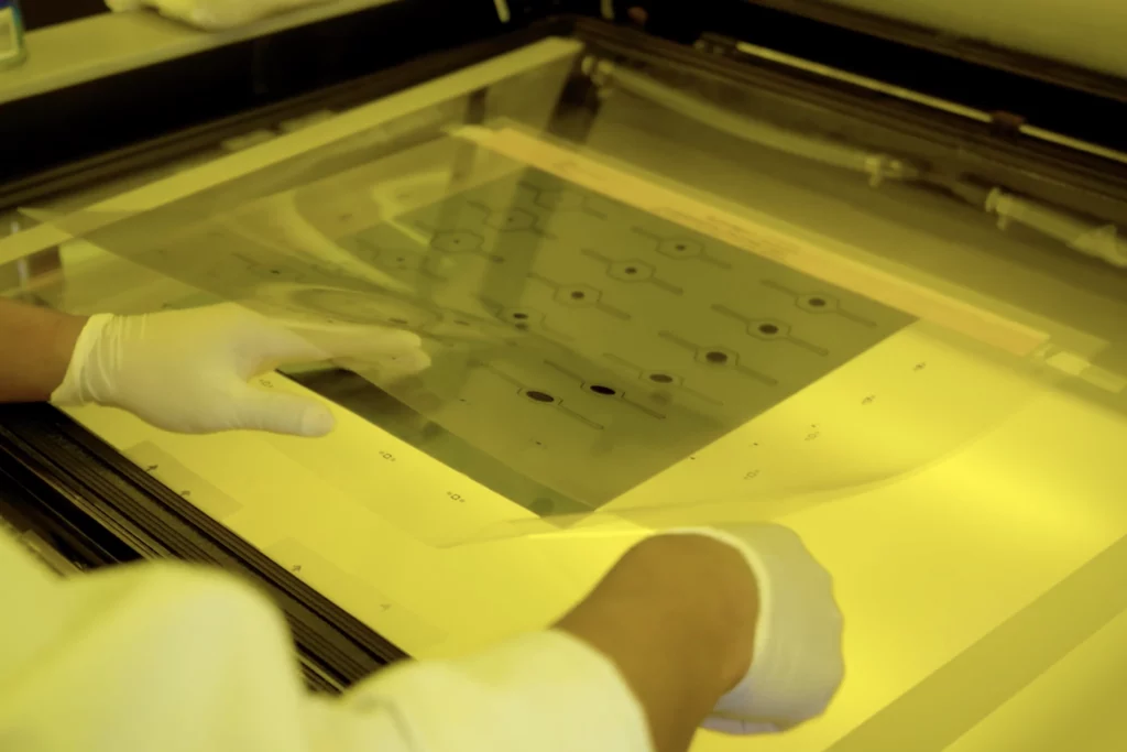
The process begins with applying a maskant (or photoresist) to the metal surface in the part’s pattern. A UV light imprints the part design onto the metal sheet, which is then developed to expose the pattern onto the metalThe chemical etchant then dissolves the exposed metal, leaving behind the desired shapes or features.
This method produces intricate and complex designs with tight tolerances, making it ideal for semiconductor applications where precision is paramount.
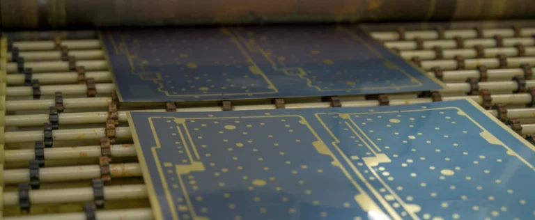
One of the key benefits of chemical etching over traditional machining methods is its versatility. Chemical etching, unlike mechanical etching or laser cutting, can be used to etch a wide range of metals, including stainless steel, copper, aluminum, and titanium, without inducing thermal stress or distortion. A cost-effective solution for high-volume production, the chemical etching process eliminates the need for expensive tooling and setup costs associated with traditional machining methods.
The Photochemical Etching Process
Benefits of Photochemical Etching for Semiconductor Components
Photochemical etching delivers numerous advantages for semiconductor components, particularly when dealing with intricate semiconductor materials.
Using a precise masking material creates complex patterns without the thermal or mechanical stress associated with dry etching or plasma etching. Unlike reactive ion etching, which can cause damage through high-energy ions, photochemical etching ensures the integrity of semiconductor diodes and other sensitive components. It also supports anisotropic etching, providing directionally uniform cuts that improve the performance of electronic devices.
Let’s take a closer look at some of the key benefits of PCE for enhancing semiconductor technology.
High Precision and Accuracy:
Photochemical etching can achieve extremely fine details with tolerances as tight as a few micrometers. This level of precision is essential for semiconductor components, where even the smallest deviation can impact performance.
Ability to Create Complex and Intricate Designs:
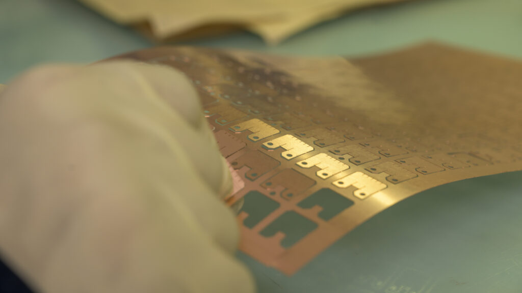
The process allows for the creation of highly intricate and complex patterns that are difficult to achieve with other methods, which is particularly beneficial for semiconductor components that require detailed microstructures.
Reduced Risk of Thermal Damage:
Unlike laser cutting, photochemical etching does not involve high temperatures, eliminating the risk of thermal distortion or damage to the material. This preserves the material’s properties and enhances component reliability.
Consistency and Repeatability in Production:
Our Photochemical etching process uses the direct digital imager which allows for precise design alignment, providing consistent and repeatable results across large production runs and ensuring that each component meets specifications. This repeatability is crucial for maintaining quality and performance in semiconductor manufacturing.
E-Fab’s Expertise in Photochemical Etching
E-Fab is a leading manufacturer specializing in photochemical etching services. Boasting decades of experience and a portfolio of successful projects, E-Fab has developed expertise in delivering high-quality precision components for various applications.
We use industry-leading photochemical machining equipment, and our innovative processes and expert staff ensure that every component we fabricate is of the highest quality.
Semiconductor OEMs rely on us to help them solve complex design, machining, and part assembly needs from prototype to completion. We can meet the demand for precise, complex, and feature-rich metal semiconductor parts and components with the highest levels of accuracy and repeatability, which is vital due to the critical nature of semiconductor applications. Our semiconductor photo etching capabilities allow us to fabricate high-precision metal parts that are complex and multi-layered.
As material selection specialists, we work with a wide range of metals and alloys, including, but not limited to, tungsten, molybdenum, copper, stainless steel, Kovar, and nickel. We can also use dielectric and insulating materials when components with specific electrical or thermal insulation properties are required.
Improving Semiconductor Component Quality
Due to the high precision and intricate detailing achievable with photochemical etching, several critical semiconductor components benefit from improved quality, performance, and reliability in various electronic applications.
The main ways photochemical etching significantly enhances the quality of semiconductor components include:
- Precision and Uniformity: Photochemical etching’s high precision and accuracy ensure that each component is manufactured to exact specifications, reducing variability and enhancing performance.
- Complex Geometries: The ability to create complex and intricate designs allows for the development of advanced semiconductor components with enhanced functionality.
- Material Integrity: Photochemical etching maintains the integrity of the material by avoiding thermal damage, leading to more durable and reliable components.
The consistency and repeatability of photochemical etching also ensure that each component meets stringent quality standards, leading to highly reliable semiconductor devices essential for advanced electronic applications.
Semiconductor Components Enhanced Through Photochemical Etching:
A wide range of semiconductor components benefit from the high precision and intricate detailing achievable with photochemical etching, leading to improved performance and reliability in various electronic applications. Some of these components include:
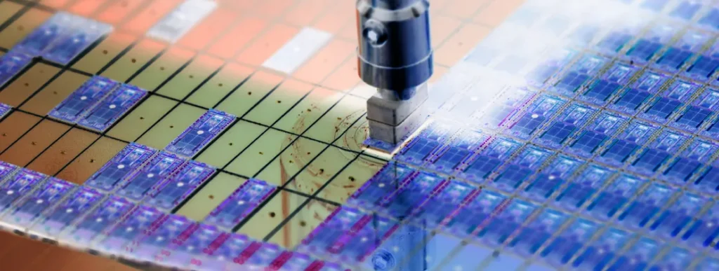
- Microelectromechanical Systems (MEMS): These tiny devices, used in sensors and actuators, benefit from the precision and intricate detailing possible with photochemical etching.
- Integrated Circuits (ICs): The ability to create fine, detailed patterns ensures that ICs function correctly and efficiently, with minimal defects.
- Lead Frames: Precise etching that ensures reliable electrical connections is crucial for lead frames used in semiconductor packaging.
E-Fab can deliver precision semiconductor photo etching services that produce intricate and complex parts and components that achieve ultra-precise dimensional and structural tolerances and high conductivity for long service life and improved yields. Fabricating a wide variety of semiconductor parts, such as contacts, maps, splits, apertures, clips, springs, connectors, and EMI/RFI shielding, we deliver high-precision metal parts that are complex and multi-layered.
Enhancing the Performance and Reliability of Semiconductor Devices
With photochemical etching, E-Fab manufactures semiconductor components with high precision, complex designs, and a reduced risk of thermal damage. By enhancing the quality, performance, and reliability of these critical components, this proven manufacturing process is shaping the future of modern technology by redefining what’s possible.
As the demand for high-quality semiconductors continues to grow, so will the demand for this innovative manufacturing technique. Thus, it is more critical than ever to partner with a manufacturer with a proven track record of delivering precision, photochemically etched semiconductor components and parts.
As specialists in photochemical etching, the team at E-Fab can deliver the precision metal etching required for achieving high-quality semiconductor devices. As an ISO 9001:2015 certified company, we offer a unique combination of advanced technology, proven production processes, engineering expertise, and value-added secondary services, allowing us to provide innovative solutions to complex jobs and unique design challenges for semiconductor parts and components.
Talk to us today for precision, quality and consistency in semiconductor manufacturing.