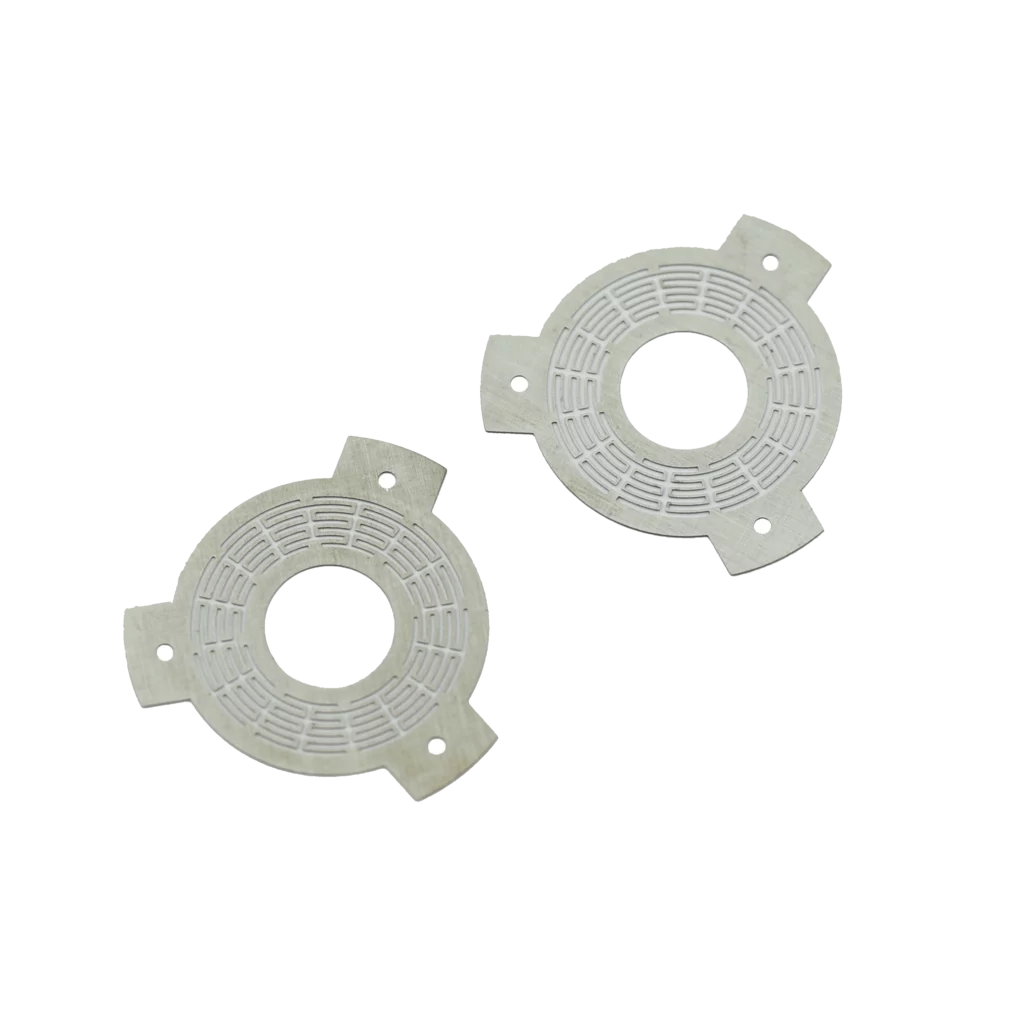
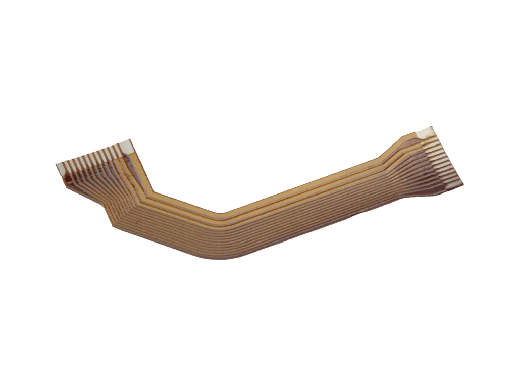
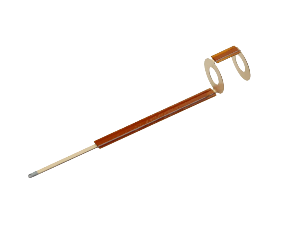
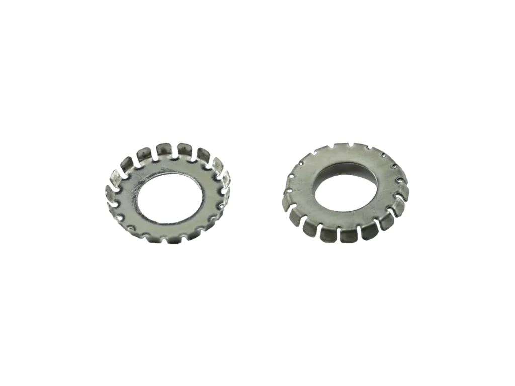
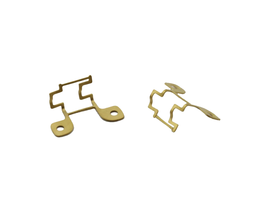
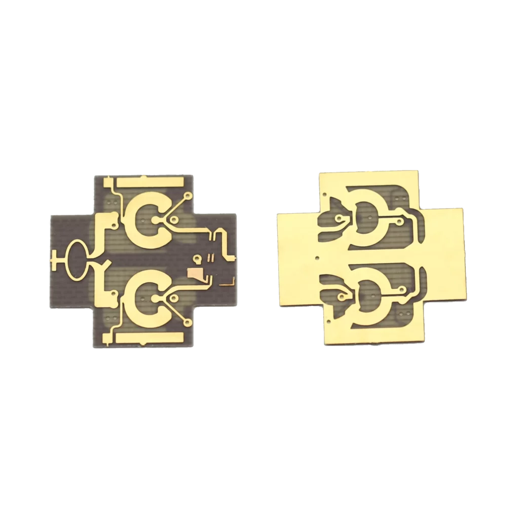
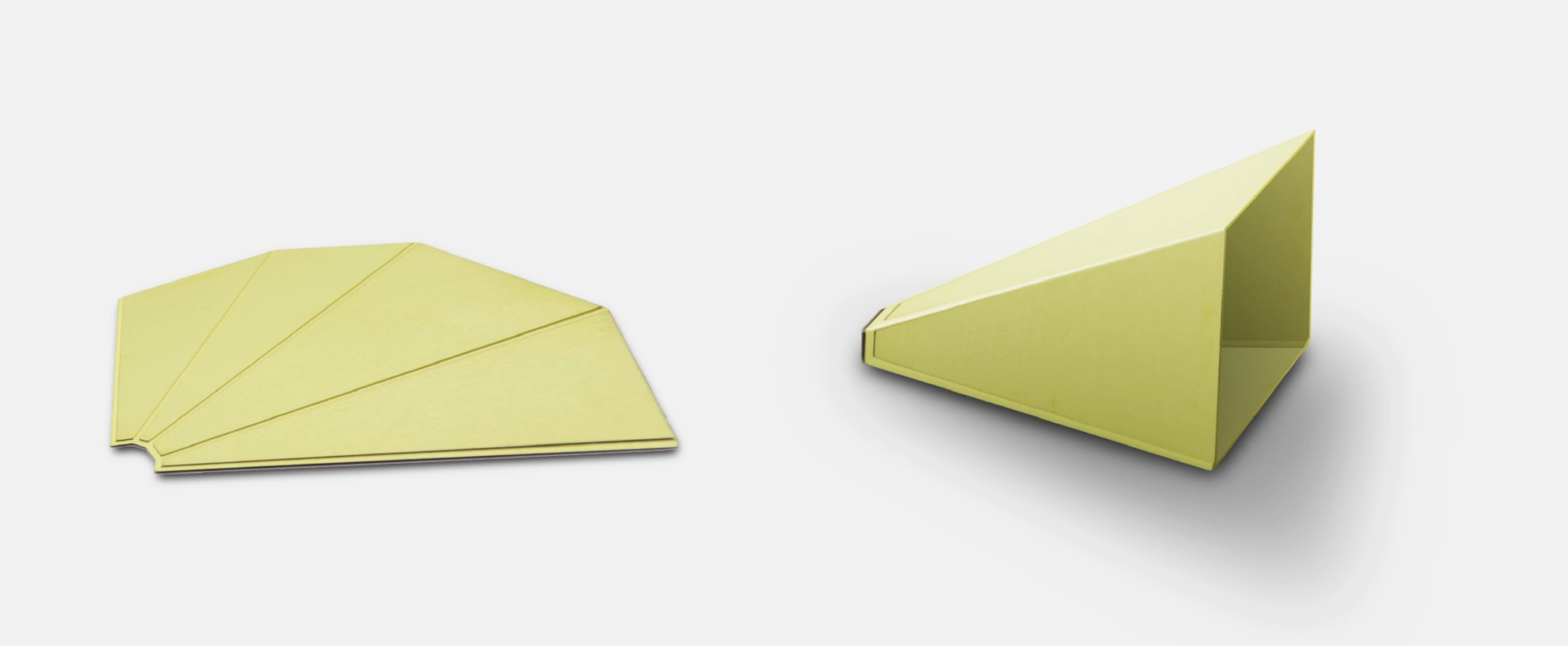
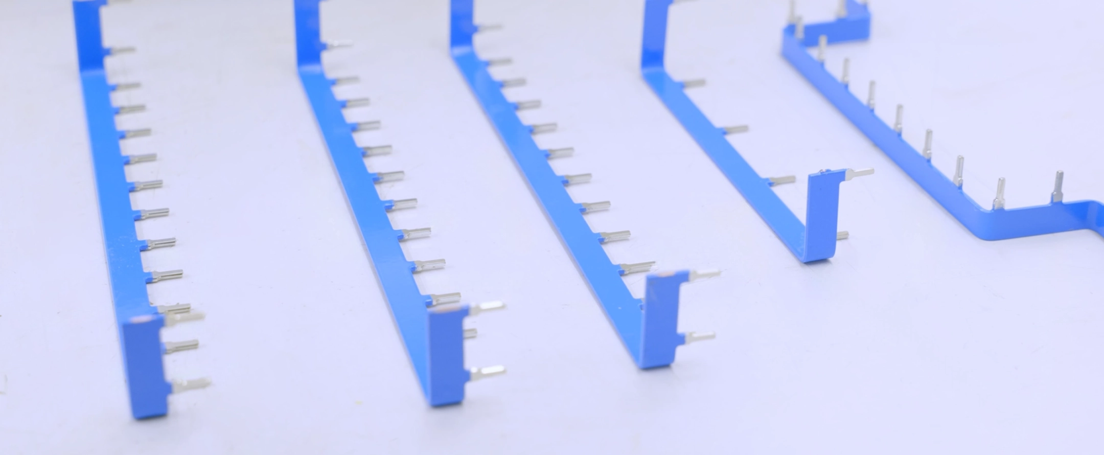
E-Fab Photo Chemical Machining News


E-FAB Is Hiring - Click Here


Bookmark and Share


Engineers, E-FAB accepts all major credit cards and can get started immediately with your prototype orders. Contact E-FAB today.


Google
Web E-FAB.COM


DXZone


E-FAB Antenna Fab


E-FAB Photo Chemical Machining, Photo Chemical Etching
Advanced Machining Micro CNC Alternatives

Metal Etching Micro Photo Fabrication

CNC Machining Manufacturing FAB Alternatives

Photo Etching Technologies, Hybrid Circuits, Mil Spec Projects, Swiss Ultra Precision Parts Manufacturing Procedures. Check out our Formed Micro Bumps Switch Contacts.


Technology terms defined: Photo Chemical Machining (PCM), photo etching, and chemical milling involves the exact removal of material from a thin metal sheet by various processes. The thin metal parts can then be formed into a variety of complex shapes. The photo chemical machining and milling processes can precisely etch lines and spaces on all types of metals (alloys: kovar, nickel, brass, beryllium, copper, stainless steel, aluminum, and others) with detailed accuracies. This is process is also used for creating specialty flex circuits, plus in engineering of other flex/rigid and rigid technologies. This results in a burr free part with very close tolerances. Take a detailed view of the fabricated antenna elements example part for details to what can be produced using this technology.

Manufacturing engineering design

E-FAB, Inc. provides customer support through all project phases.

We've helped our customers engineer special applications & products from the prototype design and development phases, then carried the project through to mass production work. There have been numerous specially engineered development, hybrid & mil-spec work projects that are of a proprietary nature which are being used in diverse industries. Through our technical and engineering support we can help you in your designs.

Precision Formed Micro Bumps

IC Test Sockets

Read more about the formed micro bumps for switch contact points for various types of contact point applications.

Parts Manufacturer Fabrication List

The following is a small PCM products sampling listing various types of precision high quality burr free, chemically machined components, provided for customers.


  • Space Fed Lens Antennas
  • Space Borne Etched Antenna Membranes
  • Machined forming dies formed contacts.
  • Milling, etched RFID tracker antenna fabrication geometries arrays, teflon bonding.
  • Engineering change orders: flexible jumpers traces.
  • Specialty FAB, flex circuits, leadframes.
  • Interconnect interposers for stacked memory devices and other components.
  • RF shields power EMI/RFI shielding.
  • Lids, step lids for hybrid packages.
  • Screens, filter mesh screen. Filters for fine particulates & EMI RFI mesh screens.
  • Printed circuit board heat sinks, PCB jumpers, shims, stiffeners, carriers, thermal layers, planes, frames.
  • Dielectric coated copper conductors.
  • Insulated contact, non-insulated contacts.
  • Precise manufacturing of specialized tooling.
  • Etched encoder disks, encoder strips.
  • Etched ultra precision metal scales.
  • Semiconductor lead frames.
  • Gimbals springs.
  • Surface mount solder screening stencils.
  • Bus bars.
  • Actuator bands.
  • Miniature ornaments & decorative designs etching.
  • shielding photo etching
  • Etched septum filter inserts.
  • Complex shaped thin metal widgets.
  • Serving the following Industries:

    Serving the aerospace, communications, computer, defense, electronic, hybrid circuits, rigid flexible circuit, interconnect, laser, dental, medical, instrumentation, micro electric circuits, microwave, military, ordinance, optical, power semiconductor, semiconductors, RFID and RF microwave antenna fabrication, interconnect interposers for stacked memory modules, tactical, weapons systems, plus other high tech OEMs.


    Utilizing photo chemical machining, photo etching, chemical milling, and CNC micro fabrication techniques for close tolerance manufacturing procedures have many possibilities in producing a wide variety of precision parts & components. Our staff is in place for help in engineering, prototype design, & mass production phases on diverse types of etched part projects. Our engineers will gladly take the time & evaluate your design requirements. For prompt delivery, superior quality, prototypes, and development projects are welcome; contact E FAB800.600.3322

    Fine Screen Mesh For RFI & EMI Filters And Fine Particle Filters

    Micro chemical machining, photo-etching, & milling projects. No etching job is too small or too big for E-FAB.

    Chemical Machining and Engineering Terminology | E-Fab Santa Clara, CA - Map Location | Privacy Policy | SiteMap

    The machining of thin metal parts made of copper, beryllium copper, brass, bronze, tin, nickel, nickel silver, molybdenum, steel, stainless steel, spring steels, aluminum, magnetic alloys, Duroid laminates, polyimides, Teflons, ceramic substrates, Kovar, and other common and exotic materials are all ideally suited to be fabricated using the photo chemical machining and photo etch processes.


    Bookmark and Share


    Copyright © 2009 E-FAB All rights reserved
    All trademarks, registered trademarks, servicemarks, and copyrights are the property of their respective holders.

    Precision thin metal parts photo-etching at E-FAB.


    Precision Bent Thin Metal Parts


     EMI RFI PCB Shielding


    Etched Antennas


    Bookmark and Share